Fabrication of UTAF
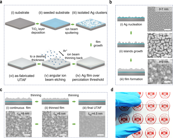
The three-dimensional (3D) flow chart in Fig. 1a schematically demonstrates the thinning-back process for UTAF fabrication. First, a titanium oxide (TiOx) layer is coated on substrates before an Ag film is deposited (Fig. 1aii), which serves as the dielectric seed layer to enhance the wettability of the deposited Ag film. To obtain full and uniform coverage of the seed layer on substrates, an atomic layer deposition technique is used here. Then, a thicker Ag film is deposited by ion beam sputtering (IBS). At the beginning stage of IBS deposition, many isolated Ag clusters are obtained on the seeded substrates due to incomplete wetting (Fig. 1aiii). Via proceeding with the deposition, a sufficiently continuous Ag film is deposited for the subsequent thinning back (Fig. 1aiv) when the deposited thickness is over the percolation threshold. Subsequently, the deposited film is thinned back via angular ion beam polishing (Fig. 1av). Eventually, a UTAF with a desired thickness is achieved (Fig. 1avi). To obtain an excellent UTAF, both high-quality deposition and thinning are key procedures in our developed process. Due to the mismatch of surface energy, Ag adatoms on substrates tend to form tiny dots as nucleation sites (Fig. 1bi) at the beginning of the deposition, even promoted by TiOx seed layer. However, enabled by the additional kinetic energy of the deposited atoms in the IBS process, surface diffusion of Ag adatoms promotes the lateral growth of dots. With the continuous deposition, the tiny dots gradually grow up to islands, coalesce into nanodroplets (Fig. 1bii), merge to connected channels, further form a porous film, and eventually achieve a continuous and dense film with a small thickness (Fig. 1biii). To ensure the process more reliable, the thickness of deposited Ag should be 1â2ânm thicker than the percolation threshold. Note that the percolation threshold can be tuned by the wettability of Ag with changing different wetting layers. For example, the percolation threshold for a TiOx-seeded UTAF can decrease from 12 to 9ânm (Supplementary Fig. 1) compared to that of the unseeded UTAF. Based on the as-prepared Ag film (Fig. 1ci), after the subsequent angular etching, the thickness of the Ag film can be reduced to 8, 6, and 4.5ânm. When the film is further thinned to be 3ânm, its morphology becomes discontinuous and changes to be particle shape (Supplementary Fig. 2), though it is still electrically conductive. Moreover, the film surface can be polished by selective planarization of the topographic peaks (Fig. 1cii). With the polishing, the surface roughness is improved (Supplementary Fig. 3). Eventually, a continuous Ag film can be fabricated with a desired thinness and a smooth surface (Fig. 1ciii). To verify the advantages of IBS, we also conducted the thinning-back process based on the magnetron-sputtered and thermally evaporated Ag films. The thinnest achievable thickness of continuous Ag for magnetron sputtering and thermal evaporation were larger than 5.5 and 10.5ânm, respectively (Supplementary Fig. 4), indicating that the IBS technique for Ag deposition is the preferable method to achieve the ultimate thinness. As a proof of concept, a 4.5-nm-thick Ag film is fabricated on a polyethylene terephthalate (PET) plate using this method, and this thin Ag film exhibits high transparency to the naked eye, as shown in Fig. 1d.
a 3D schematics showing the ion-beam thinning-back process flow in UTAF fabrication. b Series of schematic diagrams exhibiting the detailed growth process of Ag film using the IBS technique. The inset SEM images from top to bottom present the morphologies at nominal thicknesses of 1, 4, and 9ânm. c Serial schemes showing the thinning-back and polishing process of the Ag film using glancing ion beam etching with a given incident angle referring to sample surface. The inset SEM images from left to right demonstrate the topography evolution of the Ag film with reduced thicknesses of 8, 6 and 4.5ânm. d Photograph of 4.5-nm-thick UTAF on a PET plate (60âmm à 35âmm). Scale bars are 50ânm for all insets in panels (b, c).
Morphological analysis of UTAF
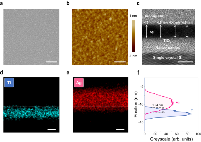
Based on this process, a continuous Ag film can be thinned back down to 4.5ânm, which is the thinnest one until now. The detailed morphology of the film is investigated, as shown in Fig. 2. In Fig. 2a, long-range continuity of the Ag film without voids is observed in scanning electron microscopy (SEM) images. In contrast, disconnected morphology is observed in the directly deposited film (i.e., without the thinning-back process) with the same thickness (Supplementary Fig. 5). Atomic force microscopy (AFM) analysis further shows the roughness Rq is as low as 0.18ânm, as shown in Fig. 2b. No pit defect is probed using AFM mapping. Cross-sectional transmission electron microscopy (TEM) is used to gain insight into the internal structure of the UTAF. As shown in Fig. 2c, the thickness of seeded Ag film is 4.5â±â0.1ânm. The uniform greyscale in the Ag region depicts no internal porous defects, and the absence of lattice fringes means that an amorphous film is obtained, which benefits the realization of a smooth surface due to the mitigated anisotropic etching of nanocrystals with different facets. The geometrical thickness measured by TEM is also consistent with the optical thickness (4.6ânm) determined by spectroscopic ellipsometry with angstrom resolution, which confirms the long-range uniformity of the UTAF over a large area. The thickness variation at the 1âà scale indicates the atomical smoothness of the film. To explore the cause of the stability of such thin Ag film, the Ag/TiOx interface analysis is performed. In Fig. 2d, e, energy-dispersive X-ray spectrometry (EDS) in the scanning TEM mode is applied to probe the element distribution. Line-scan mapping (Fig. 2d, e) suggests the occurrence of interface intermixing between Ag and TiOx, i.e., a part of Ag atoms penetrate into the TiOx seed layer. Through the statistics of Ag and Ti signals, an intermixing depth of 1.94ânm (Fig. 2f) was measured, which indicates the generation of Ag implantation in the early stage of Ag film deposition.
a Electron micrograph of the surface morphology. Scale bar: 200ânm. b Corresponding AFM topography mapping with a scanning resolution of 512âÃâ512 pixels in a 1âÃâ1âμm2 area. Scale bar: 200ânm. c Cross-sectional TEM image of a 4.5-nm-thick UTAF. Scale bar: 5ânm. d, e EDS mappings of Ti and Ag elements in the scanning TEM mode, respectively. Scale bars: 2ânm. f Signal analysis for Ag and Ti distributions at the interface. The signals are extracted from the greyscale integration of corresponding EDS mapping images in panels d and e.
Implantation effect
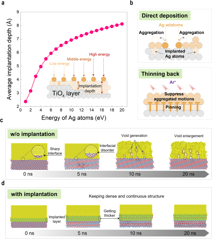
To further understand the implantation effect in the fabrication of UTAF, systematic simulations were executed. In the stage of IBS deposition, the energy of Ag atoms ejected from the target is dispersive. These Ag atoms with changing energy projecting into the TiOx underlayer would form an implantation layer on the top of the interface (Fig. 3a inset). Through the Stopping and Range of Ions in Matter (SRIM)29 simulations, the maximal energy of Ag atoms ejected by 500-eV Ar+ bombardment is determined to be ~19.8âeV. Figure 3a shows that the average implantation depth for the maximal energy of Ag atoms is 8âà . The energy dispersion result in a continuous implantation region at the interface, which can serve as a buffer layer to mitigate the aggregation of Ag adatoms induced by the cohesive energy. Even so, the challenge of realizing long-range continuity of UTAF with direct deposition process using the IBS technique remains. In the early stage of IBS deposition, the discontinuity of the Ag implanted layer cannot provide sufficient wettability to expand Ag adatoms into a continuous film because the number of the implanted Ag atoms is not sufficient (top inset in Fig. 3b). Enabled by thinning-back process, a continuous implantation layer is formed when the Ag film over the percolation threshold is deposited using IBS deposition. Empowered by the continuous implantation layer, the âpinning effectâ can suppress the dewetting behavior caused by disordered thermal motions of Ag atoms when the UTAF is thinned back to 4.5ânm (bottom inset in Fig. 3b). Such âpinning effectâ is crucial for achieving long-range continuity in UTAFs. Molecular dynamics (MD) simulations further confirm the âpinning effectâ on UTAFs, as shown in Fig. 3c and d. In the absence of implantation (Fig. 3c), the part of the Ag matrix close to the interface becomes disordered at the start of the MD simulation (5âns). Then, the disordered arrangement of Ag atoms spreads to the whole matrix, and the continuous matrix changes to grain-like structures with voids generation (10âns). With the proceeding of the disordered thermal motions at 300âK, voids in the matrix are enlarged, finally forming porous defects (20âns). In the presence of implantation (labeled by green areas, Fig. 3d), the part of the ordered Ag matrix lying on TiOx close to the interface merely appears to change in arrangement, and the implanted layer becomes large in depth. The Ag matrix remains dense and continuous during the whole process of the simulation, which confirms that the âpinning effectâ induced by implantation can stabilize UTAFs at the ultimate thinness.
a Calculated average implantation depth of ejected Ag atoms into TiOx underlayer as a function of the kinetic energy in SRIM software. The kinetic energy of the Ag atom is in the range of 1â20âeV with an increment of 1âeV. The average implantation depth is the mean value of the vertical projection range from 106 Ag atoms in the single calculation. Inset scheme demonstrates Ag implantation with various kinetic energies during the IBS deposition. b Schematic showing the different behavior of Ag adatoms in UTAF fabrication using direct deposition and thinning-back processes. c, d MD simulation showing the structural evolution of the ordered-arrangement Ag matrix without and with interface implantation at 300âK, respectively.
Optical and electrical characteristics
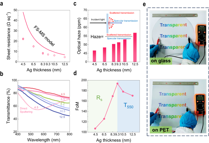
The superior long-range continuity and excellent surface roughness of UTAFs obtained enable high performance in terms of transparency and electrical conductivity. Here, the visible transmittance and sheet resistance of a seeded UTAF with a reduced thickness during thinning back are measured, as shown in Fig. 4a, b. For a thin metal film, a higher resistivity for thinner films is mainly ascribed to electron scattering from the surface. The process can be explained by the FuchsâSondheimer (FS)30,31 and MayadasâShatzkes (MS)32,33 models. Here, a comparison of Rs values of UTAFs and fitting data based on the FSâMS model34 is shown in Fig. 4a. All of the UTAF samples exhibit overall superiority to the equivalents in the FSâMS model. Moreover, the difference between UTAFs and the FSâMS model becomes larger with decreasing Ag thickness (tAg), which is consistent with the change in surface roughness for thinned UTAFs in Supplementary Fig. 3.
a Rs for UTAFs with changing reduced thicknesses during thinning back. Raw data (hollow dots) of Rs from five random positions are extracted for each sample. The line fit is the plot of Rs of Ag films in the FS-MS model. b Corresponding measured visible transmittance of UTAFs. Solid lines represent continuous UTAFs. The tAg values labeled on solid lines is the optical thickness measured by ellipsometry. The dashed line represents the particle-shaped UTAF fabricated by direct deposition using the IBS technique. c Average visible haze of the UTAFs with different thickness. The inset shows the principle and calculation of optical haze for a film. d FoM of UTAFs with changing reduced thickness tAg. e Photographs of 9-nm-thick UTAFs on a 12-inch glass wafer (top panel) and a 300âÃâ300 mm2 PET plate (bottom panel).
The measured transmittance for thinned UTAFs exhibits a coincident downward trend in the visible range and becomes progressively lower at longer wavelengths with increasing tAg (Fig. 4b), which confirms the sufficient continuity of UTAFs down to tAgâ=â4.5ânm. The lower visible transmittance at longer wavelengths makes UTAFs a gray-blue color, similar to low-emission glass. In contrast, the Ag film directly deposited by IBS presents a transmittance dip at approximately λâ=â548ânm, which is attributed to localized surface plasmon resonance of discontinuous metallic islands35. The distinctive spectral behavior of the dashed line verifies the infeasibility of using direct deposition to reduce a continuous Ag film down to 4.5ânm. To provide a direct evaluation of the transparency, the average transmittance (Tavg) integrated into the visible range is introduced. For tAgâ=â4.5ânm, Tavg can reach 82%, which is greater than that of commercial ITO (Tavgâ=â77%)36. Tavg for the discontinuous 4.5-nm-thick (nominal value) Ag film produced via direct IBS deposition is just 63%. As the UTAF thickness increases, Tavg drastically decreases to 62% in the case of tAgâ=â12.5ânm (Supplementary Table 1). In addition to the long-range continuity, the atomic-scale roughness further suppresses the optical loss caused by scattering and realizes extremely low transmission haze. As shown in Fig. 4c, the integrated haze in the visible range is less than 60 ppm for all UTAF samples, and its value gradually decreased due to the improved smoothness as the Ag thickness tAg is reduced by the thinning-back step. X-ray diffraction characterization indicates that the improved smoothness is also related to the amorphous nature of the Ag film with thinner thickness (Supplementary Fig. 6). The extremely low optical haze promotes the collimation of transmissive light, which greatly improves the efficacy of light-emitting devices. To assess the overall performance of UTAFs as a transparent conductor, FoM is commonly used as a quantitative index37. Figure 4d plots the FoM of the obtained UTAFs. With increasing tAg, the FoM has an optimal value (194) in the case of tAgâ=â9ânm. Applying the two derived variables Rs(tAg) and T550(tAg) in the FoM function38 188.5/(RsÃ(T550-1/2-1)), we find that the increase of FoM is predominated by the decrease of Rs in the range of 4.5ânmâ¤tAgââ¤â9ânm (green area). For tAgââ¥â9ânm (blue area), the severe deterioration in T550 dominantly affects the down slope of the FoM. As a demonstration of this process on uniform large-area fabrication, UTAFs fabricated on a glass wafer (12-inch) and a polymer plate (300âÃâ300 mm2) exhibit the potential to be TCF candidates (Fig. 4e). The low sheet resistance (7.7âΩâsqâ1 on glass; 7.6âΩâsqâ1 on PET) illustrates the high continuity of the demonstrated UTAFs. The underlying full color âTransparentâ words present high fidelity in hues, which indicates high transparency in the visible range. Furthermore, the aging test of UTAF is executed as well. Lasting for a week, the stable transparency and electrical conductivity indicate that UTAFs have the potential to be a promising candidate of ITO alternatives (Supplementary Fig. 7, Table 2).
Mechanical tests
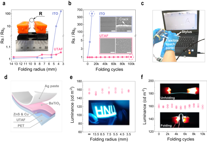
Contributed from the ductility of metals, UTAFs on polymers are promising candidates for flexible transparent conductors. Here, their flexibility is systemically evaluated. Using a desktop unit for flexibility testing (inset in Fig. 5a), a robust mechanical tensile strength is exhibited by folding a 9-nm-thick UTAF on PET to different curvature radii (R). For the minimal radius Râ=â3.5âmm, Rs merely increases by 5% (Fig. 5a). For the commercial flexible ITO, Rs drastically increases to 155 times of the original value. In addition to the static strength test, the dynamic fatigue lifetime further demonstrates their flexibility for practical applications. In the cyclic folding test, Rs for UTAF only has a slight increase of 6.58% after 105 cycles. For commercial ITO, the sheet resistance is 601 times larger than the original value after 104 cycles. Morphology characterization clarifies that the drastic degradation of electrical conductance for ITO is ascribed to the presence of massive through cracks (Supplementary Fig. 8). In contrast, UTAF keep a continuous surface during the whole test. The excellent mechanical flexibility permits UTAFs as a promising ITO alternative for flexible optoelectronic devices. Here, we demonstrate a flexible resistive touch panel made of two parallel UTAFs (tAgâ=â9ânm) on PET with an air gap. As shown in Fig. 5c, the letter âAâ can be clearly written on the folded touch panel.
a Static flexibility of a 9-nm-thick UTAF with different folding radii. The inset photograph presents of the flexibility test unit. b Folding stability of the electrical conductance of a 9-nm-thick UTAF and commercial ITO within 105 cycles. Insets show the SEM images and photographs of the ITO and UTAF after 104 cycles and 105 cycles, respectively. Scale bars in insets: 25 μm in left photographs; 100ânm in right SEM images. c Proof-of-concept demonstration of a foldable resistive touch panel. d 3D scheme for the configuration of a foldable ACEL device. e Luminance plot of a foldable ACEL device with changing folding curvature. The ACEL device is driven by a sinusoidal signal (160âV, 16âkHz). The inset picture shows a folded ACEL device with an HNU logo. f Luminance stability of the ACEL device undergoing a cyclic folding test. Inset images present the unfolding and folding states for the working ACEL device.
Flexible light-emitting devices
With the excellent mechanical flexibility and high transmittance, UTAFs can serve as flexible transparent electrodes for foldable light-emitting devices. In Fig. 5dâf, we demonstrate a foldable alternating current electroluminescent (ACEL) device application using flexible transparent electrodes based on a 9-nm-thick UTAF on PET. Figure 5d presents the configuration of a foldable ACEL device. The flexible ACEL device consists of multiple layers in the following order: a UTAF on PET (bottom electrode), zinc sulfur (ZnS) mixed with copper (Cu) nanoparticles (active layer, ~40âμm), barium titanate (BaTiO3, dielectric layer, ~20âμm), and a top Ag electrode (Ag paste, ~20âμm). When subjected to the folding test, the foldable ACEL maintains a luminance of 160âcdâmâ2 when it is folded with changing curvature radius in static conditions, as shown in Fig. 5e. The electroluminescence (EL) stability of the foldable ACEL device is exhibited by a cyclic folding test (Fig. 5f). After 104 folding cycles, the EL intensity remains at 160âcdâmâ2. For the foldable device, the UTAF provides excellent mechanical flexibility as a uniform carrier collector to support a stable EL intensity over a large area.
In summary, we have developed an ion-beam-based thinning-back strategy to push the thinness limit of a continuous Ag film down to 4.5ânm. Simulations indicate that the shallow implantation capability of the ion-beam-sputtered atoms and the pinning-effect of the implanted atoms are responsible for the improved stability of the UTAFs. With this thinning-back strategy, the final UTAFs exhibit long-range continuity and atomic-level roughness, enabling enhanced transparency and ultimate transmission haze. When combined with polymer substrates, the UTAFs demonstrate robust mechanical stability as a flexible transparent conductor, which boosts the steady EL performance of foldable light-emitting devices. Suitable capping layer can be used to mitigate the oxidization and simultaneously serve as an antireflection (Supplementary Fig. 9, Table 3) or functional device film8,19. Appreciating its ultimate capability, we believe that this ion-beam-based thinning-back strategy has the potential to be a general approach capable of producing large-area UTAFs for flexible optoelectronics. Meanwhile, this thinning-back strategy could be extended to fabricate other ultrathin functional films, such as ultrasmooth Au films for low-loss plasmonics, the multilayer reflector for short-wavelength optics, and superconductive films in quantum science.


